Right Now

HVPE GaN Single Crystal Substrate Research:CAGR of 12.30% during the forecast period
HVPE GaN Single Crystal Substrate Product Introduction
HVPE GaN single crystal substrate refers to a self-supporting GaN single crystal substrate obtained by peeling or polishing by growing high-quality GaN single crystal thick film on GaN seed crystal substrate using hydride vapor phase epitaxy (HVPE) technology. It does not need to rely on heterogeneous substrates such as sapphire and silicon carbide for support. It has low defect density, high crystal quality, thermal stability, high thermal conductivity and high breakdown voltage. It is suitable for high-performance optoelectronic devices (LED/LD), power electronic devices, high-frequency electronic devices and other fields.
HVPE GaN Single Crystal Substrate Market Summary
According to the new market research report “Global HVPE GaN Single Crystal Substrate Market Report 2025-2031”, published by QYResearch, the global HVPE GaN Single Crystal Substrate market size is projected to reach USD 0.37 billion by 2031, at a CAGR of 12.30% during the forecast period.
Figure00002. Global HVPE GaN Single Crystal Substrate Market Size (US$ Million), 2020-2031
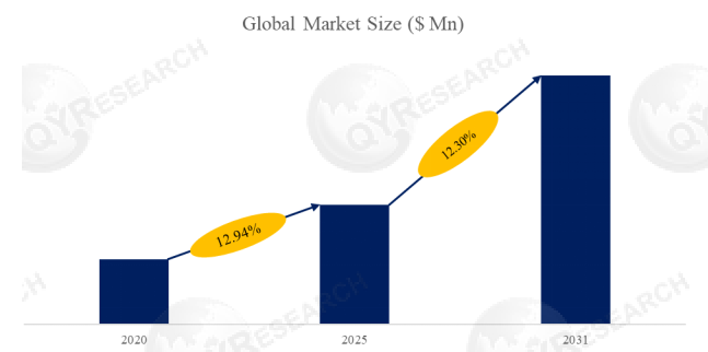
Above data is based on report from QYResearch: Global HVPE GaN Single Crystal Substrate Market Report 2025-2031 (published in 2025). If you need the latest data, plaese contact QYResearch.
Figure00003. Global HVPE GaN Single Crystal Substrate Top 10 Players Ranking and Market Share (Ranking is based on the revenue of 2024, continually updated)
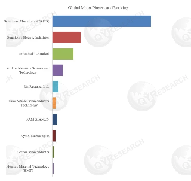
Above data is based on report from QYResearch: Global HVPE GaN Single Crystal Substrate Market Report 2025-2031 (published in 2025). If you need the latest data, plaese contact QYResearch.
According to QYResearch Top Players Research Center, the global key manufacturers of HVPE GaN Single Crystal Substrate include Sumitomo Chemical (SCIOCS), Sumitomo Electric Industries, Mitsubishi Chemical, Suzhou Nanowin Science and Technology, etc. In 2024, the global top four players had a share approximately 83.70% in terms of revenue, the global top three players had a share approximately 78.18% in terms of revenue.
Figure00004. HVPE GaN Single Crystal Substrate, Global Market Size, Split by Product Segment
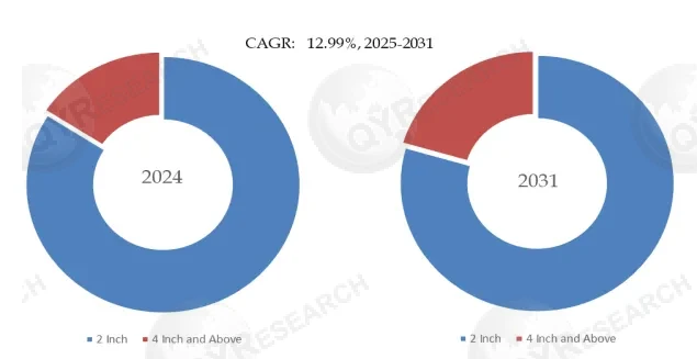
Based on or includes research from QYResearch: Global HVPE GaN Single Crystal Substrate Market Report 2025-2031.
In terms of product type, currently 2 Inch is the largest segment, hold a share of 84.14%.
In terms of product application, currently Optoelectronics is the largest segment, hold a share of 70.07%.
Industry Trends:
Main Development Trends
Preparation of high-quality, large-size single crystal substrates: With the increasing demand for high-efficiency gallium nitride (GaN)-based semiconductor devices, especially in the fields of LED, power electronics and 5G communications, the development of large-size, high-quality GaN single crystal substrates has become a research focus. The HVPE method is expected to produce larger-size GaN single crystal substrates to meet the growing market demand by improving epitaxial growth technology and optimizing gas phase reaction conditions. Sumitomo Chemical and other companies have achieved mass production of 4-inch GaN substrates and accelerated the development of 6-inch substrate commercialization technology.
Increasing growth rate and reducing costs: By optimizing gas flow, temperature control and adding auxiliary materials during the HVPE process, researchers are increasing the growth rate of GaN substrates, thereby reducing costs and improving production efficiency. With the continuous advancement of technology, the production cost of the HVPE method is expected to gradually decrease, further promoting its application in the commercial market.
Optimization of doping technology: Improve electrical properties through doping with Mg, Fe, C, etc., meet the needs of power devices and RF devices, and reduce unintentional doping (Si, O) to improve material purity.
Cost reduction and large-scale production: Improvement of HVPE equipment (such as reaction chamber design and by-product control) improves growth efficiency.
Restraint:
Fluctuations in Growth Quality and Defects: Although the HVPE method has great advantages in the preparation of GaN single crystal substrates, in actual production, problems such as inhomogeneity, defects, cracks or dislocations may occur during the growth process. These defects not only affect the electronic and optical properties of GaN, but also limit its large-scale commercial application.
Difficulty in the production of large-size substrates: Although the HVPE method can produce GaN single crystals well, the preparation of large-size, high-quality single crystal substrates is still a technical challenge. At present, the production of large-size GaN single crystal substrates is still in the exploratory stage, and the related problems of equipment and processes need to be further solved. Stress control and uniformity of 6-inch and above substrates are still facing challenges.
Costly equipment and technical requirements: Although the HVPE method can prepare high-quality GaN single crystal substrates, the investment and operation costs of the equipment are high, especially in the context of large-scale production. The maintenance and operation of HVPE equipment requires precise technical support and high-cost investment. In addition, the complexity of HVPE equipment and low yield also lead to the price of GaN single crystal substrates being much higher than other heterogeneous substrates such as SiC and Si.
International competition and patent barriers: Leading companies such as Japan's Sumitomo Chemical dominate the market and have a technology monopoly. Companies in other countries still rely on imports for core equipment and processes.
Opportunity:
Demand for 5G and high-performance electronic devices: With the promotion of 5G communication technology, the advantages of GaN materials in high-power and high-frequency applications are becoming more and more significant. GaN single crystal substrates prepared by HVPE are widely used in 5G base stations, radar systems, high-efficiency power devices and other fields, and the market demand is growing rapidly.
Expansion of LED and laser markets: GaN materials are widely used in high-brightness LEDs and lasers. With the continuous development of display technology and the lighting industry, the demand for high-performance GaN single crystal substrates continues to increase. HVPE GaN single crystal substrates will benefit from this market trend.
Application of electric vehicles and power semiconductor devices: With the development of green energy technologies such as electric vehicles and smart grids, GaN power semiconductors are widely used in power conversion and power electronic devices in electric vehicles due to their high efficiency and high voltage resistance. The HVPE method can provide high-quality GaN single crystal substrates for these devices, further expanding market applications.
Material innovation and technological progress: Current research focuses on improving the quality and large-scale production of GaN single crystal substrates. With the innovation of material science and HVPE process, the technical barriers of GaN single crystal substrates will be gradually broken, opening up more opportunities for the future market.
Environmental friendliness and sustainable development: High-efficiency GaN semiconductor materials can improve energy efficiency and have a wide range of applications in green energy and environmental protection technologies. With the improvement of environmental protection requirements, the application of GaN materials will occupy an increasingly important position in the fields of environmental protection and energy, and HVPE GaN single crystal substrates will be favored.
About QYResearch
QYResearch founded in California, USA in 2007.It is a leading global market research and consulting company. With over 18 years’ experience and professional research team in various cities over the world QY Research focuses on management consulting, database and seminar services, IPO consulting (data is widely cited in prospectuses, annual reports and presentations), industry chain research and customized research to help our clients in providing non-linear revenue model and make them successful. We are globally recognized for our expansive portfolio of services, good corporate citizenship, and our strong commitment to sustainability. Up to now, we have cooperated with more than 60,000 clients across five continents. Let’s work closely with you and build a bold and better future.
QYResearch is a world-renowned large-scale consulting company. The industry covers various high-tech industry chain market segments, spanning the semiconductor industry chain (semiconductor equipment and parts, semiconductor materials, ICs, Foundry, packaging and testing, discrete devices, sensors, optoelectronic devices), photovoltaic industry chain (equipment, cells, modules, auxiliary material brackets, inverters, power station terminals), new energy automobile industry chain (batteries and materials, auto parts, batteries, motors, electronic control, automotive semiconductors, etc.), communication industry chain (communication system equipment, terminal equipment, electronic components, RF front-end, optical modules, 4G/5G/6G, broadband, IoT, digital economy, AI), advanced materials industry Chain (metal materials, polymer materials, ceramic materials, nano materials, etc.), machinery manufacturing industry chain (CNC machine tools, construction machinery, electrical machinery, 3C automation, industrial robots, lasers, industrial control, drones), food, beverages and pharmaceuticals, medical equipment, agriculture, etc.
Contact Us:
If you have any queries regarding this report or if you would like further information, please contact us:
QY Research Inc.
Add: 17890 Castleton Street Suite 369 City of Industry CA 91748 United States
EN: https://www.qyresearch.com
Email: global@qyresearch.com
Tel: 001-626-842-1666(US)
JP: https://www.qyresearch.co.jp
More Posts


Report This Post
Please complete the following requested information to flag this post and report abuse, or offensive content. Your report will be reviewed within 24 hours. We will take appropriate action as described in Findit terms of use.