Right Now

Electron Beam Metrology & Inspection Equipment Industry Research
Semiconductor Metrology & Inspection Equipment runs through every process of wafer manufacturing, from design verification to process control detection to wafer testing and finished product testing. Metrology & Inspection Equipment plays a vital role in controlling and improving the yield of wafer manufacturing. According to the testing link, semiconductor Metrology & Inspection can be divided into front-end inspection and back-end inspection. Front-end Metrology & Inspection occurs in the wafer preparation and silicon wafer manufacturing process, including the Metrology of various film thicknesses, nanostructure critical dimensions (CD), overlay errors and other dimensional parameters formed in the silicon wafer manufacturing process, and wafer surface defects, to ensure that the yield of the processing line is controlled above the specified level. According to different functions, front-end Metrology & Inspection equipment is divided into Metrology and defect inspection. The former is mainly for film thickness, film stress, critical dimensions, doping concentration, etc., and the latter is mainly used for wafer surface defect inspection, which is one of the keys to process control and yield management in semiconductor manufacturing.
The purpose of defect inspection is to accurately identify, locate and classify key defects (DOI, which refers to any defect type that is considered to have an impact on yield, reliability or performance) on the inspected wafer, thereby helping defect and yield engineers to quickly resolve defect problems, which is of great significance for wafer fabs to reduce production costs and improve wafer yield.
Electron Beam Metrology & Inspection Equipment plays a vital role in semiconductor manufacturing, and is mainly used for inspection of physical defects and electrical defects of wafers and integrated circuits, as well as the size Metrology of key graphics. These devices use electron beams to scan the wafers to be tested, obtain high-resolution electron beam images, and use different algorithms to analyze information such as defects and key dimensions on the wafers.
Electron Beam Metrology & Inspection Equipment includes three core equipments, each of which realizes precise control in semiconductor manufacturing through differentiated algorithms: DR-SEM performs sampling positioning based on the defect coordinates provided by optical detection, and completes defect authenticity identification and classification verification by collecting high-resolution SEM images; Electron beam wafer defect inspection equipment (EBI) adopts full scanning detection mode, batch acquires SEM images in the specified area according to the preset detection formula, and uses intelligent analysis algorithms to directly identify and classify micron to nanometer physical/potential defects; CD-SEM focuses on precise size control, accurately reaches the preset measurement coordinates through the automatic focus system, and after collecting images of specific areas, uses pixel-level computing technology to achieve nanometer-level measurement of key structural parameters such as line width and aperture, and feeds back the measurement data to the process equipment in real time to form a closed-loop control. The three types of equipment respectively undertake the functions of defect review, comprehensive screening and precise measurement through algorithm optimization, and jointly build a quality assurance system for advanced semiconductor processes.
According to the new market research report "Electron Beam Metrology & Inspection Equipment - Global Market Share and Ranking, Overall Sales and Demand Forecast 2025-2031", published by QYResearch, the global Electron Beam Metrology & Inspection Equipment market size is projected to grow from USD 3,127 million in 2024 to USD 4,962 million by 2031, at a CAGR of 6.75% during the forecast period.
Figure00001. Global Electron Beam Metrology & Inspection Equipment Market Size (US$ Million), 2019-2030
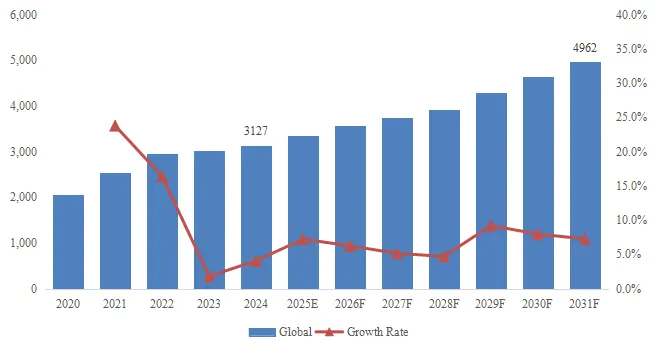
Source: QYResearch, "Electron Beam Metrology & Inspection Equipment - Global Market Share and Ranking, Overall Sales and Demand Forecast 2025-2031”
Figure00002. Global Electron Beam Metrology & Inspection Equipment Top 11 Players Ranking and Market Share (Ranking is based on the revenue of 2024, continually updated)
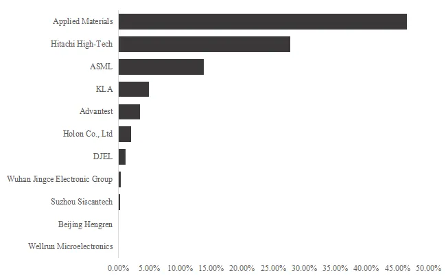
Source: QYResearch, "Electron Beam Metrology & Inspection Equipment - Global Market Share and Ranking, Overall Sales and Demand Forecast 2025-2031”
From the production side, the core production areas of Electron Beam Metrology & Inspection Equipment are mainly the United States, Europe, Japan and China, among which the United States is the main production area, accounting for 46.5% of the market share in 2024. There are still large differences between Chinese Electron Beam Metrology & Inspection Equipment companies and international leading companies (such as Applied Materials and Hitachi High-Tech) in the application, technology, and product performance of advanced support fields. However, as the localization process of Chinese local manufacturers accelerates, some Chinese local companies have also gained a certain market share in the electron beam inspection and measurement equipment market, such as Jingce Electronic and DJEL. In addition, in recent years, there have been many new entrants from Chinese local enterprises, such as Wellrun Microelectronics, Suzhou Siscantech, Beijing Hengren, Wuxi Genxinyue Technology Co., Ltd, Suzhou AISTech, etc. However, at present, their scale is relatively small or some are still in the Demo stage. With the future development of China's semiconductor market, it is expected that the global competitive share of Chinese local manufacturers will gradually increase in the next few years, and China will maintain the fastest growth rate. With the advancement of China's Electron Beam Metrology & Inspection Equipment technology, the emergence of cost advantages and the strengthening of policy support, it is expected that the share will reach 4.9% in 2031.
At present, electron beam inspection equipment (EBI and DR-SEM) accounts for the largest proportion, accounting for 73.8% of the market share in 2024. Among them, EBI is a relatively advanced equipment, and the global leading companies are mainly Applied Materials and ASML. As Chinese local front-end measurement and inspection equipment manufacturers gradually commercialize mass production, the growth rate of CD-SEM sales in the future will exceed the global growth rate, that is, the CAGR (2025-2031) will reach 6.87%.
About The Authors
Jiashi Dong
Lead Author
Email: dongjiashi@qyresearch.com
BM of QYResearch Nanning Research Center is also a key member of the semiconductor equipment and materials department of QYResearch. The main research areas include electronics, semiconductor equipment, materials, etc. Some of the sub-research topics include automotive diodes, automotive inductors, LiDAR, RF power supplies, discrete devices, Molding System, wafer defect detection and review equipment, 3D wafer AOI, precursors, electroplating equipment, semiconductor chemical plating solution, motors for semiconductor equipment, air bearing stages for semiconductor equipment, dry pumps for semiconductor equipment, semiconductor coating devices, etc. At the same time, it is also engaged in the development of market segmentation reports and participates in the writing of customized projects. Cooperating customers include Huawei, WalterFuse, Hitachi High-Tech, Towa, Mitsubishi Electric, HORIBA, Schaeffler, etc.
About QYResearch
QYResearch founded in California, USA in 2007.It is a leading global market research and consulting company. With over 17 years’ experience and professional research team in various cities over the world QY Research focuses on management consulting, database and seminar services, IPO consulting (data is widely cited in prospectuses, annual reports and presentations), industry chain research and customized research to help our clients in providing non-linear revenue model and make them successful. We are globally recognized for our expansive portfolio of services, good corporate citizenship, and our strong commitment to sustainability. Up to now, we have cooperated with more than 60,000 clients across five continents. Let’s work closely with you and build a bold and better future.
QYResearch is a world-renowned large-scale consulting company. The industry covers various high-tech industry chain market segments, spanning the semiconductor industry chain (semiconductor equipment and parts, semiconductor materials, ICs, Foundry, packaging and testing, discrete devices, sensors, optoelectronic devices), photovoltaic industry chain (equipment, cells, modules, auxiliary material brackets, inverters, power station terminals), new energy automobile industry chain (batteries and materials, auto parts, batteries, motors, electronic control, automotive semiconductors, etc.), communication industry chain (communication system equipment, terminal equipment, electronic components, RF front-end, optical modules, 4G/5G/6G, broadband, IoT, digital economy, AI), advanced materials industry Chain (metal materials, polymer materials, ceramic materials, nano materials, etc.), machinery manufacturing industry chain (CNC machine tools, construction machinery, electrical machinery, 3C automation, industrial robots, lasers, industrial control, drones), food, beverages and pharmaceuticals, medical equipment, agriculture, etc.
Contact Us:
If you have any queries regarding this report or if you would like further information, please contact us:
QY Research Inc.
Add: 17890 Castleton Street Suite 369 City of Industry CA 91748 United States
E-mail: global@qyresearch.com
Tel: 001-626-842-1666(US) 0086-133 1872 9947(CN)
More Posts


Report This Post
Please complete the following requested information to flag this post and report abuse, or offensive content. Your report will be reviewed within 24 hours. We will take appropriate action as described in Findit terms of use.